
당신은 주제를 찾고 있습니까 “built in potential – Electronic Devices: pn junction under equilibrium – depletion width, build-in potential“? 다음 카테고리의 웹사이트 th.taphoamini.com 에서 귀하의 모든 질문에 답변해 드립니다: th.taphoamini.com/wiki. 바로 아래에서 답을 찾을 수 있습니다. 작성자 techgurukula 이(가) 작성한 기사에는 조회수 105,843회 및 좋아요 1,003개 개의 좋아요가 있습니다.
Table of Contents
built in potential 주제에 대한 동영상 보기
여기에서 이 주제에 대한 비디오를 시청하십시오. 주의 깊게 살펴보고 읽고 있는 내용에 대한 피드백을 제공하세요!
d여기에서 Electronic Devices: pn junction under equilibrium – depletion width, build-in potential – built in potential 주제에 대한 세부정보를 참조하세요
built in potential 주제에 대한 자세한 내용은 여기를 참조하세요.
PN Junction Theory for Semiconductor Diodes
The significance of this built-in potential across the junction, is that it opposes both the flow of holes and electrons across the junction and is why it is …
Source: www.electronics-tutorials.ws
Date Published: 3/10/2021
View: 8740
1. Joining p – MIT OpenCourseWare
Depletion and built-in voltage. 3. Current-voltage characteristics of the p-n junction. Questions you should be able to answer by the end of today’s lecture …
Source: ocw.mit.edu
Date Published: 8/18/2021
View: 3782
p–n junction – Wikipedia
A p–n junction is a boundary or interface between two types of semiconductor materials, … This potential difference is called built-in potential V b i …
Source: en.wikipedia.org
Date Published: 10/5/2022
View: 5209
How is a built-in potential developed in a p-n junction? – Quora
Built in Potential is developed in PN juntion due to concentration gradient. P type has majority carrier Holes and N type has majority carrier as an …
Source: www.quora.com
Date Published: 9/23/2022
View: 5010
Lecture06-pn Junction (with appendix).pdf
Built-in Voltage. • At pn junction, free electrons from n-se. “recombine” with free holes from p-se. • “Depletion region” has no electrons or holes,.
Source: inst.eecs.berkeley.edu
Date Published: 11/20/2021
View: 2573
주제와 관련된 이미지 built in potential
주제와 관련된 더 많은 사진을 참조하십시오 Electronic Devices: pn junction under equilibrium – depletion width, build-in potential. 댓글에서 더 많은 관련 이미지를 보거나 필요한 경우 더 많은 관련 기사를 볼 수 있습니다.
주제에 대한 기사 평가 built in potential
- Author: techgurukula
- Views: 조회수 105,843회
- Likes: 좋아요 1,003개
- Date Published: 2015. 5. 12.
- Video Url link: https://www.youtube.com/watch?v=Ihu0zC7d7hU
What is built in potential?
In a p–n junction, without an external applied voltage, an equilibrium condition is reached in which a potential difference forms across the junction. This potential difference is called built-in potential .
What is built in potential voltage?
What is the built-in voltage Vbi? Built-in voltage is simply the difference of the Fermi levels in p- and n-type semiconductors before they were joined.
What is built in potential barrier?
This potential barrier will always exist even if the device is not connected to any external power source, as seen in diodes. The significance of this built-in potential across the junction, is that it opposes both the flow of holes and electrons across the junction and is why it is called the potential barrier.
What is built in potential of diode?
For silicon diodes, the built-in potential is approximately 0.7 V (0.3 V for germanium and 0.2 V for Schottky). Thus, if an external voltage greater than and opposite to the built-in voltage is applied, a current will flow and the diode is said to be “turned on” as it has been given an external forward bias.
How do you find built-in potential?
Built-in potential calculator uses Built-in Potential = Thermal Voltage*ln((Acceptor concentration*Donor concentration)/(Intrinsic Electron Concentration^2)) to calculate the Built-in Potential, The Built-in potential formula is defined as the built-in potential in a semiconductor equals the potential across the …
How the built-in potential is formed in pn junction?
P-n junctions are formed by joining n-type and p-type semiconductor materials, as shown below. Since the n-type region has a high electron concentration and the p-type a high hole concentration, electrons diffuse from the n-type side to the p-type side.
What does of built-in potential depend on?
Detailed Solution. So built-in potential depends on both doping densities & temperature.
Is barrier potential and built-in potential same?
Caused by a diffusion process across the pn-junction there is a “barrier” consisting of a potential difference (called voltage). This “built-in voltage” causes the diffusion to stop at a certain equlibrium. Hence, “barrier voltage” and “built-in voltage” are two different expressions for the same quantity.
What is contact potential?
the potential generated by the contact of two dissimilar materials in air or in a vacuum.
What is barrier potential in transistor?
This region of electric field keeps electrons from moving from n to p and is the potential barrier that exists across semiconductor devices. In particular, in enhancement MOSFETs the potential barrier impedes diffusion both from source to the substrate and from drain to the substrate.
What is potential barrier in diode?
A) The potential barrier in the p-n junction diode is the barrier which does not allow charge flow across the junction normally. This barrier is created by the charge present in the space charge region.
What is junction barrier potential?
The potential barrier in the p-n junction is a type of barrier which does not allow the normal flow of charge across the junction and this resistance to the flow of charge is known as barrier potential.
Why pn junction is called a diode?
Why is p-n-junction is also called a junction diode ? Solution : A p-n-junction allows a large current to flow through it when forward biased and it offers a high resistance when reverse biased. The unidirectional property is similar to that of vacuum diode. Hence, p-n-junction is also called a junction diode.
Which is called intrinsic semiconductor?
What are Intrinsic Semiconductors? Semiconductors that are chemically pure, in other words, free from impurities are termed as intrinsic semiconductors. The number of holes and electrons is therefore determined by the properties of the material itself instead of the impurities.
Why is PN junction used?
A p-n junction diode allows electric current when it is forward biased and blocks electric current when it is reverse biased. This action of p-n junction diode enables us to use it as a rectifier.
What is contact potential?
the potential generated by the contact of two dissimilar materials in air or in a vacuum.
What is contact potential in pn junction?
Thus, an electric field is formed going from the n-side to the p-side and there is a built-in potential, from the p to the n side. This potential is called the junction potential or contact potential.
What is diffusion potential in semiconductor?
Diffusion potential or the built-in potential across the p-n junction is given by: ⇒ V b i = k T q ln If the temperature is constant, the diffusion potential is ∝ ln (Na Nd) ∴ The built-in potential, across a p-n junction, increases with increases in doping concentration.
What is difference between potential barrier and depletion region?
This in turn, produces potential barrier VB across the junction which opposes the further diffusion through the junction. Thus, small region forms in the vicinity of i the junction which is depleted of free charge carrier and has only immobile ions is called the depletion regions.
PN Junction Theory for Semiconductor Diodes
This tutorial about PN junction theory shows that when silicon is doped with small amounts of Antimony, an N-type semiconductor material is formed, and when the same silicon material is doped with small amounts of Boron, a P-type semiconductor material is formed.
This is all well and good, but these newly doped N-type and P-type semiconductor materials do very little on their own as they are electrically neutral. However, if we join (or fuse) these two semiconductor materials together they behave in a very different way as they merge together producing what is generally known as a “PN Junction” allowing us to study the effect of PN junction theory.
When the N-type semiconductor and P-type semiconductor materials are first joined together a very large density gradient exists between both sides of the PN junction. The result is that some of the free electrons from the donor impurity atoms begin to migrate across this newly formed junction to fill up the holes in the P-type material producing negative ions.
However, because the electrons have moved across the PN junction from the N-type silicon to the P-type silicon, they leave behind positively charged donor ions ( N D ) on the negative side and now the holes from the acceptor impurity migrate across the junction in the opposite direction into the region where there are large numbers of free electrons.
As a result, the charge density of the P-type along the junction is filled with negatively charged acceptor ions ( N A ), and the charge density of the N-type along the junction becomes positive. This charge transfer of electrons and holes across the PN junction is known as diffusion. The width of these P and N layers depends on how heavily each side is doped with acceptor density N A , and donor density N D , respectively.
This process continues back and forth until the number of electrons which have crossed the junction have a large enough electrical charge to repel or prevent any more charge carriers from crossing over the junction. Eventually a state of equilibrium (electrically neutral situation) will occur producing a “potential barrier” zone around the area of the junction as the donor atoms repel the holes and the acceptor atoms repel the electrons.
Since no free charge carriers can rest in a position where there is a potential barrier, the regions on either sides of the junction now become completely depleted of any more free carriers in comparison to the N and P type materials further away from the junction. This area around the PN Junction is now called the Depletion Layer.
The PN junction
The total charge on each side of a PN Junction must be equal and opposite to maintain a neutral charge condition around the junction. If the depletion layer region has a distance D, it therefore must therefore penetrate into the silicon by a distance of Dp for the positive side, and a distance of Dn for the negative side giving a relationship between the two of: Dp*N A = Dn*N D in order to maintain charge neutrality also called equilibrium.
Depletion Layer Distance
As the N-type material has lost electrons and the P-type has lost holes, the N-type material has become positive with respect to the P-type. Then the presence of impurity ions on both sides of the junction cause an electric field to be established across this region with the N-side at a positive voltage relative to the P-side. The problem now is that a free charge requires some extra energy to overcome the barrier that now exists for it to be able to cross the depletion region junction.
This electric field created by the diffusion process has created a “built-in potential difference” across the junction with an open-circuit (zero bias) potential of:
Where: E o is the zero bias junction voltage, V T the thermal voltage of 26mV at room temperature, N D and N A are the impurity concentrations and n i is the intrinsic concentration.
A suitable positive voltage (forward bias) applied between the two ends of the PN junction can supply the free electrons and holes with the extra energy. The external voltage required to overcome this potential barrier that now exists is very much dependent upon the type of semiconductor material used and its actual temperature.
Typically at room temperature the voltage across the depletion layer for silicon is about 0.6 – 0.7 volts and for germanium is about 0.3 – 0.35 volts. This potential barrier will always exist even if the device is not connected to any external power source, as seen in diodes.
The significance of this built-in potential across the junction, is that it opposes both the flow of holes and electrons across the junction and is why it is called the potential barrier. In practice, a PN junction is formed within a single crystal of material rather than just simply joining or fusing together two separate pieces.
The result of this process is that the PN junction has rectifying current–voltage (IV or I–V) characteristics. Electrical contacts are fused onto either side of the semiconductor to enable an electrical connection to be made to an external circuit. The resulting electronic device that has been made is commonly called a PN junction Diode or simply Signal Diode.
Then we have seen here in this tutorial about PN junction theory, that PN junctions can be made by joining or diffusing together differently doped semiconductor materials to produce an electronic device called a diode which can be used as the basic semiconductor structure of rectifiers, all types of transistors, LED’s, solar cells, and many more such solid state devices.
In the next tutorial about the PN junction, we will look at one of the most interesting applications of the PN junction is its use in circuits as a diode. By adding connections to each end of the P-type and the N-type materials we can produce a two terminal device called a PN Junction Diode which can be biased by an external voltage to either block or allow the flow of current through it.
p–n junction
Semiconductor–semiconductor junction
A p–n junction. The circuit symbol is shown: the triangle corresponds to the p side.
A p–n junction is a boundary or interface between two types of semiconductor materials, p-type and n-type, inside a single crystal of semiconductor. The “p” (positive) side contains an excess of holes, while the “n” (negative) side contains an excess of electrons in the outer shells of the electrically neutral atoms there. This allows electrical current to pass through the junction only in one direction. The p-n junction is created by doping, for example by ion implantation, diffusion of dopants, or by epitaxy (growing a layer of crystal doped with one type of dopant on top of a layer of crystal doped with another type of dopant). If two separate pieces of material were used, this would introduce a grain boundary between the semiconductors that would severely inhibit its utility by scattering the electrons and holes.[citation needed]
p–n junctions are elementary “building blocks” of semiconductor electronic devices such as diodes, transistors, solar cells, LEDs, and integrated circuits; they are the active sites where the electronic action of the device takes place. For example, a common type of transistor, the bipolar junction transistor, consists of two p–n junctions in series, in the form n–p–n or p–n–p; while a diode can be made from a single p-n junction. A Schottky junction is a special case of a p–n junction, where metal serves the role of the n-type semiconductor.
Properties [ edit ]
The p–n junction possesses a useful property for modern semiconductor electronics. A p-doped semiconductor is relatively conductive. The same is true of an n-doped semiconductor, but the junction between them can become depleted of charge carriers, and hence non-conductive, depending on the relative voltages of the two semiconductor regions. By manipulating this non-conductive layer, p–n junctions are commonly used as diodes: circuit elements that allow a flow of electricity in one direction but not in the other (opposite) direction.
Bias is the application of a voltage relative to a p–n junction region:
forward bias is in the direction of easy current flow
is in the direction of easy current flow reverse bias is in the direction of little or no current flow.
The forward-bias and the reverse-bias properties of the p–n junction imply that it can be used as a diode. A p–n junction diode allows electric charges to flow in one direction, but not in the opposite direction; negative charges (electrons) can easily flow through the junction from n to p but not from p to n, and the reverse is true for holes. When the p–n junction is forward-biased, electric charge flows freely due to reduced resistance of the p–n junction. When the p–n junction is reverse-biased, however, the junction barrier (and therefore resistance) becomes greater and charge flow is minimal.
Equilibrium (zero bias) [ edit ]
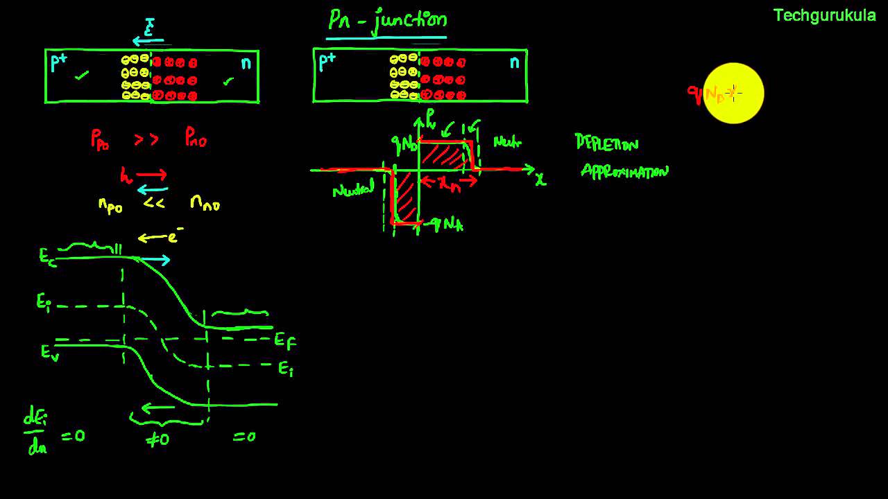
In a p–n junction, without an external applied voltage, an equilibrium condition is reached in which a potential difference forms across the junction. This potential difference is called built-in potential V b i {\displaystyle V_{\rm {bi}}} .
At the junction, some of the free electrons in the n-type wander into the p-type due to random thermal migration. As they diffuse into the p-type they combine with holes, and cancel each other out. In a similar way some of the positive holes in the p-type wander into the n-type and combine with free electrons, and cancel each other out. The positively charged, donor, dopant atoms in the n-type are part of the crystal, and cannot move. Thus, in the n-type, a region near the junction becomes positively charged. The negatively charged, acceptor, dopant atoms in the p-type are part of the crystal, and cannot move. Thus, in the p-type, a region near the junction becomes negatively charged. The result is a region near the junction that acts to repel the mobile charges away from the junction through the electric field that these charged regions create. The regions near the p–n interface lose their neutrality and most of their mobile carriers, forming the space charge region or depletion layer (see figure A).
Figure A. A p–n junction in thermal equilibrium with zero-bias voltage applied. Electron and hole concentration are reported with blue and red lines, respectively. Gray regions are charge-neutral. Light-red zone is positively charged. Light-blue zone is negatively charged. The electric field is shown on the bottom, the electrostatic force on electrons and holes and the direction in which the diffusion tends to move electrons and holes. (The log concentration curves should actually be smoother with slope varying with field strength.) A p–n junction in thermal equilibrium with zero-bias voltage applied. Electron and hole concentration are reported with blue and red lines, respectively. Gray regions are charge-neutral. Light-red zone is positively charged. Light-blue zone is negatively charged. The electric field is shown on the bottom, the electrostatic force on electrons and holes and the direction in which the diffusion tends to move electrons and holes. (The log concentration curves should actually be smoother with slope varying with field strength.)
The electric field created by the space charge region opposes the diffusion process for both electrons and holes. There are two concurrent phenomena: the diffusion process that tends to generate more space charge, and the electric field generated by the space charge that tends to counteract the diffusion. The carrier concentration profile at equilibrium is shown in figure A with blue and red lines. Also shown are the two counterbalancing phenomena that establish equilibrium.
Figure B. A p–n junction in thermal equilibrium with zero-bias voltage applied. Under the junction, plots for the charge density, the electric field, and the voltage are reported. (The log concentration curves should actually be smoother, like the voltage.) A p–n junction in thermal equilibrium with zero-bias voltage applied. Under the junction, plots for the charge density, the electric field, and the voltage are reported. (The log concentration curves should actually be smoother, like the voltage.)
The space charge region is a zone with a net charge provided by the fixed ions (donors or acceptors) that have been left uncovered by majority carrier diffusion. When equilibrium is reached, the charge density is approximated by the displayed step function. In fact, since the y-axis of figure A is log-scale, the region is almost completely depleted of majority carriers (leaving a charge density equal to the net doping level), and the edge between the space charge region and the neutral region is quite sharp (see figure B, Q(x) graph). The space charge region has the same magnitude of charge on both sides of the p–n interfaces, thus it extends farther on the less doped side in this example (the n side in figures A and B).
Forward bias [ edit ]
In forward bias, the p-type is connected with the positive terminal and the n-type is connected with the negative terminal.
PN junction operation in forward-bias mode, showing reducing depletion width.
The panels show energy band diagram, electric field, and net charge density. Both p and n junctions are doped at a 1e15/cm3 (0.00016C/cm3) doping level, leading to built-in potential of ~0.59 V. Reducing depletion width can be inferred from the shrinking carrier motion across the p–n junction, which as a consequence reduces electrical resistance. Electrons that cross the p–n junction into the p-type material (or holes that cross into the n-type material) diffuse into the nearby neutral region. The amount of minority diffusion in the near-neutral zones determines the amount of current that can flow through the diode.
Only majority carriers (electrons in n-type material or holes in p-type) can flow through a semiconductor for a macroscopic length. With this in mind, consider the flow of electrons across the junction. The forward bias causes a force on the electrons pushing them from the N side toward the P side. With forward bias, the depletion region is narrow enough that electrons can cross the junction and inject into the p-type material. However, they do not continue to flow through the p-type material indefinitely, because it is energetically favorable for them to recombine with holes. The average length an electron travels through the p-type material before recombining is called the diffusion length, and it is typically on the order of micrometers.[1]
Although the electrons penetrate only a short distance into the p-type material, the electric current continues uninterrupted, because holes (the majority carriers) begin to flow in the opposite direction. The total current (the sum of the electron and hole currents) is constant in space, because any variation would cause charge buildup over time (this is Kirchhoff’s current law). The flow of holes from the p-type region into the n-type region is exactly analogous to the flow of electrons from N to P (electrons and holes swap roles and the signs of all currents and voltages are reversed).
Therefore, the macroscopic picture of the current flow through the diode involves electrons flowing through the n-type region toward the junction, holes flowing through the p-type region in the opposite direction toward the junction, and the two species of carriers constantly recombining in the vicinity of the junction. The electrons and holes travel in opposite directions, but they also have opposite charges, so the overall current is in the same direction on both sides of the diode, as required.
The Shockley diode equation models the forward-bias operational characteristics of a p–n junction outside the avalanche (reverse-biased conducting) region.
Reverse bias [ edit ]
A silicon p–n junction in reverse bias.
Connecting the p-type region to the negative terminal of the voltage supply and the n-type region to the positive terminal corresponds to reverse bias. If a diode is reverse-biased, the voltage at the cathode is comparatively higher than at the anode. Therefore, very little current flows until the diode breaks down. The connections are illustrated in the adjacent diagram.
Because the p-type material is now connected to the negative terminal of the power supply, the ‘holes’ in the p-type material are pulled away from the junction, leaving behind charged ions and causing the width of the depletion region to increase. Likewise, because the n-type region is connected to the positive terminal, the electrons are pulled away from the junction, with similar effect. This increases the voltage barrier causing a high resistance to the flow of charge carriers, thus allowing minimal electric current to cross the p–n junction. The increase in resistance of the p–n junction results in the junction behaving as an insulator.
The strength of the depletion zone electric field increases as the reverse-bias voltage increases. Once the electric field intensity increases beyond a critical level, the p–n junction depletion zone breaks down and current begins to flow, usually by either the Zener or the avalanche breakdown processes. Both of these breakdown processes are non-destructive and are reversible, as long as the amount of current flowing does not reach levels that cause the semiconductor material to overheat and cause thermal damage.
This effect is used to advantage in Zener diode regulator circuits. Zener diodes have a low breakdown voltage. A standard value for breakdown voltage is for instance 5.6 V. This means that the voltage at the cathode cannot be more than about 5.6 V higher than the voltage at the anode (though there is a slight rise with current), because the diode breaks down, and therefore conduct, if the voltage gets any higher. This, in effect, limits the voltage over the diode.
Another application of reverse biasing is Varactor diodes, where the width of the depletion zone (controlled with the reverse bias voltage) changes the capacitance of the diode.
Governing equations [ edit ]
Size of depletion region [ edit ]
For a p–n junction, let C A ( x ) {\displaystyle C_{A}(x)} be the concentration of negatively-charged acceptor atoms and C D ( x ) {\displaystyle C_{D}(x)} be the concentrations of positively-charged donor atoms. Let N 0 ( x ) {\displaystyle N_{0}(x)} and P 0 ( x ) {\displaystyle P_{0}(x)} be the equilibrium concentrations of electrons and holes respectively. Thus, by Poisson’s equation:
− d 2 V d x 2 = ρ ε = q ε [ ( P 0 − N 0 ) + ( C D − C A ) ] {\displaystyle -{\frac {\mathrm {d} ^{2}V}{\mathrm {d} x^{2}}}={\frac {\rho }{\varepsilon }}={\frac {q}{\varepsilon }}\left[(P_{0}-N_{0})+(C_{D}-C_{A})\right]}
where V {\displaystyle V} is the electric potential, ρ {\displaystyle \rho } is the charge density, ε {\displaystyle \varepsilon } is permittivity and q {\displaystyle q} is the magnitude of the electron charge.
For a general case, the dopants have a concentration profile that varies with depth x, but for a simple case of an abrupt junction, C A {\displaystyle C_{A}} can be assumed to be constant on the p side of the junction and zero on the n side, and C D {\displaystyle C_{D}} can be assumed to be constant on the n side of the junction and zero on the p side. Let d p {\displaystyle d_{p}} be the width of the depletion region on the p-side and d n {\displaystyle d_{n}} the width of the depletion region on the n-side. Then, since P 0 = N 0 = 0 {\displaystyle P_{0}=N_{0}=0} within the depletion region, it must be that
d p C A = d n C D {\displaystyle d_{p}C_{A}=d_{n}C_{D}}
because the total charge on the p and the n side of the depletion region sums to zero. Therefore, letting D {\displaystyle D} and Δ V {\displaystyle \Delta V} represent the entire depletion region and the potential difference across it,
Δ V = ∫ D ∫ q ε [ ( P 0 − N 0 ) + ( C D − C A ) ] d x d x = C A C D C A + C D q 2 ε ( d p + d n ) 2 {\displaystyle \Delta V=\int _{D}\int {\frac {q}{\varepsilon }}\left[(P_{0}-N_{0})+(C_{D}-C_{A})\right]\,\mathrm {d} x\,\mathrm {d} x={\frac {C_{A}C_{D}}{C_{A}+C_{D}}}{\frac {q}{2\varepsilon }}(d_{p}+d_{n})^{2}}
And thus, letting d {\displaystyle d} be the total width of the depletion region, we get
d = 2 ε q C A + C D C A C D Δ V {\displaystyle d={\sqrt {{\frac {2\varepsilon }{q}}{\frac {C_{A}+C_{D}}{C_{A}C_{D}}}\Delta V}}}
Δ V {\displaystyle \Delta V} can be written as Δ V 0 + Δ V ext {\displaystyle \Delta V_{0}+\Delta V_{\text{ext}}} , where we have broken up the voltage difference into the equilibrium plus external components. The equilibrium potential results from diffusion forces, and thus we can calculate Δ V 0 {\displaystyle \Delta V_{0}} by implementing the Einstein relation and assuming the semiconductor is nondegenerate (i.e., the product P 0 N 0 = n i 2 {\displaystyle {P}_{0}{N}_{0}={n}_{i}^{2}} is independent of the Fermi energy):
Δ V 0 = k T q ln ( C A C D P 0 N 0 ) = k T q ln ( C A C D n i 2 ) {\displaystyle \Delta V_{0}={\frac {kT}{q}}\ln \left({\frac {C_{A}C_{D}}{P_{0}N_{0}}}\right)={\frac {kT}{q}}\ln \left({\frac {C_{A}C_{D}}{n_{i}^{2}}}\right)}
Current across depletion region [ edit ]
whereis the temperature of the semiconductor andis Boltzmann constant
The Shockley ideal diode equation characterizes the current across a p–n junction as a function of external voltage and ambient conditions (temperature, choice of semiconductor, etc.). To see how it can be derived, we must examine the various reasons for current. The convention is that the forward (+) direction be pointed against the diode’s built-in potential gradient at equilibrium.
Forward Current ( J F {\displaystyle \mathbf {J} _{F}} Diffusion Current: current due to local imbalances in carrier concentration n {\displaystyle n} J D ∝ − q ∇ n {\displaystyle \mathbf {J} _{D}\propto -q
abla n}
Reverse Current ( J R {\displaystyle \mathbf {J} _{R}} Field Current Generation Current
Non-rectifying junctions [ edit ]
In the above diagrams, contact between the metal wires and the semiconductor material also creates metal–semiconductor junctions called Schottky diodes. In a simplified ideal situation a semiconductor diode would never function, since it would be composed of several diodes connected back-to-front in series. But, in practice, surface impurities within the part of the semiconductor that touches the metal terminals greatly reduces the width of those depletion layers, to such an extent that the metal-semiconductor junctions do not act as diodes. These non-rectifying junctions behave as ohmic contacts regardless of applied voltage polarity.
Manufacture [ edit ]
The p-n junction is created by doping, for example by ion implantation, diffusion of dopants, or by epitaxy (growing a layer of crystal doped with one type of dopant on top of a layer of crystal doped with another type of dopant). If two separate pieces of material were used, this would introduce a grain boundary between the semiconductors that would severely inhibit its utility by scattering the electrons and holes.[citation needed]
History [ edit ]
The invention of the p–n junction is usually attributed to American physicist Russell Ohl of Bell Laboratories in 1939.[3] Two years later (1941), Vadim Lashkaryov reported discovery of p–n junctions in Cu 2 O and silver sulphide photocells and selenium rectifiers.[4]
See also [ edit ]
References [ edit ]
Further reading [ edit ]
PN Junction Theory for Semiconductor Diodes
This tutorial about PN junction theory shows that when silicon is doped with small amounts of Antimony, an N-type semiconductor material is formed, and when the same silicon material is doped with small amounts of Boron, a P-type semiconductor material is formed.
This is all well and good, but these newly doped N-type and P-type semiconductor materials do very little on their own as they are electrically neutral. However, if we join (or fuse) these two semiconductor materials together they behave in a very different way as they merge together producing what is generally known as a “PN Junction” allowing us to study the effect of PN junction theory.
When the N-type semiconductor and P-type semiconductor materials are first joined together a very large density gradient exists between both sides of the PN junction. The result is that some of the free electrons from the donor impurity atoms begin to migrate across this newly formed junction to fill up the holes in the P-type material producing negative ions.
However, because the electrons have moved across the PN junction from the N-type silicon to the P-type silicon, they leave behind positively charged donor ions ( N D ) on the negative side and now the holes from the acceptor impurity migrate across the junction in the opposite direction into the region where there are large numbers of free electrons.
As a result, the charge density of the P-type along the junction is filled with negatively charged acceptor ions ( N A ), and the charge density of the N-type along the junction becomes positive. This charge transfer of electrons and holes across the PN junction is known as diffusion. The width of these P and N layers depends on how heavily each side is doped with acceptor density N A , and donor density N D , respectively.
This process continues back and forth until the number of electrons which have crossed the junction have a large enough electrical charge to repel or prevent any more charge carriers from crossing over the junction. Eventually a state of equilibrium (electrically neutral situation) will occur producing a “potential barrier” zone around the area of the junction as the donor atoms repel the holes and the acceptor atoms repel the electrons.
Since no free charge carriers can rest in a position where there is a potential barrier, the regions on either sides of the junction now become completely depleted of any more free carriers in comparison to the N and P type materials further away from the junction. This area around the PN Junction is now called the Depletion Layer.
The PN junction
The total charge on each side of a PN Junction must be equal and opposite to maintain a neutral charge condition around the junction. If the depletion layer region has a distance D, it therefore must therefore penetrate into the silicon by a distance of Dp for the positive side, and a distance of Dn for the negative side giving a relationship between the two of: Dp*N A = Dn*N D in order to maintain charge neutrality also called equilibrium.
Depletion Layer Distance
As the N-type material has lost electrons and the P-type has lost holes, the N-type material has become positive with respect to the P-type. Then the presence of impurity ions on both sides of the junction cause an electric field to be established across this region with the N-side at a positive voltage relative to the P-side. The problem now is that a free charge requires some extra energy to overcome the barrier that now exists for it to be able to cross the depletion region junction.
This electric field created by the diffusion process has created a “built-in potential difference” across the junction with an open-circuit (zero bias) potential of:
Where: E o is the zero bias junction voltage, V T the thermal voltage of 26mV at room temperature, N D and N A are the impurity concentrations and n i is the intrinsic concentration.
A suitable positive voltage (forward bias) applied between the two ends of the PN junction can supply the free electrons and holes with the extra energy. The external voltage required to overcome this potential barrier that now exists is very much dependent upon the type of semiconductor material used and its actual temperature.
Typically at room temperature the voltage across the depletion layer for silicon is about 0.6 – 0.7 volts and for germanium is about 0.3 – 0.35 volts. This potential barrier will always exist even if the device is not connected to any external power source, as seen in diodes.
The significance of this built-in potential across the junction, is that it opposes both the flow of holes and electrons across the junction and is why it is called the potential barrier. In practice, a PN junction is formed within a single crystal of material rather than just simply joining or fusing together two separate pieces.
The result of this process is that the PN junction has rectifying current–voltage (IV or I–V) characteristics. Electrical contacts are fused onto either side of the semiconductor to enable an electrical connection to be made to an external circuit. The resulting electronic device that has been made is commonly called a PN junction Diode or simply Signal Diode.
Then we have seen here in this tutorial about PN junction theory, that PN junctions can be made by joining or diffusing together differently doped semiconductor materials to produce an electronic device called a diode which can be used as the basic semiconductor structure of rectifiers, all types of transistors, LED’s, solar cells, and many more such solid state devices.
In the next tutorial about the PN junction, we will look at one of the most interesting applications of the PN junction is its use in circuits as a diode. By adding connections to each end of the P-type and the N-type materials we can produce a two terminal device called a PN Junction Diode which can be biased by an external voltage to either block or allow the flow of current through it.
Wikipedia
Electronic component that only allows current to flow in one direction
Diode Close-up view of a silicon diode. The anode is on the right side; the cathode is on the left side (where it is marked with a black band). The square silicon crystal can be seen between the two leads. Type Passive Pin configuration Anode and cathode Electronic symbol
Structure of a vacuum tube diode. The filament itself may be the cathode, or more commonly (as shown here) used to heat a separate metal tube which serves as the cathode.
A diode is a two-terminal electronic component that conducts current primarily in one direction (asymmetric conductance); it has low (ideally zero) resistance in one direction, and high (ideally infinite) resistance in the other.
A diode vacuum tube or thermionic diode is a vacuum tube with two electrodes, a heated cathode and a plate, in which electrons can flow in only one direction, from cathode to plate.
A semiconductor diode, the most commonly used type today, is a crystalline piece of semiconductor material with a p–n junction connected to two electrical terminals.[4] Semiconductor diodes were the first semiconductor electronic devices. The discovery of asymmetric electrical conduction across the contact between a crystalline mineral and a metal was made by German physicist Ferdinand Braun in 1874. Today, most diodes are made of silicon, but other semiconducting materials such as gallium arsenide and germanium are also used.[5]
Among many uses, diodes are found in rectifiers to convert AC power to DC, demodulation in radio receivers, and can even be used as temperature sensors. A common variant of a diode is a light emitting diode, which is used as electric lighting and status indicators on electronic devices. Diodes may be combined with other components to form logic gates.
Main functions [ edit ]
The most common function of a diode is to allow an electric current to pass in one direction (called the diode’s forward direction), while blocking it in the opposite direction (the reverse direction). As such, the diode can be viewed as an electronic version of a check valve. This unidirectional behavior is called rectification and is used to convert alternating current (ac) to direct current (dc). As rectifiers, diodes can be used for such tasks as extracting modulation from radio signals in radio receivers.
However, diodes can have more complicated behavior than this simple on–off action, because of their nonlinear current-voltage characteristics.[6] For instance, a diode’s forward-direction voltage drop varies only a little with the current, and is more so a function of temperature; this effect can be used as a temperature sensor or as a voltage reference. And its high resistance to current flowing in the reverse direction suddenly drops to a low resistance when the reverse voltage across the diode reaches a value called the breakdown voltage. Semiconductor diodes in the forward direction also need to surpass a threshold voltage, or cut-in voltage, before being able to conduct electricity.
A semiconductor diode’s current–voltage characteristic can be tailored by selecting the semiconductor materials and the doping impurities introduced into the materials during manufacture.[6] These techniques are used to create special-purpose diodes that perform many different functions.[6] For example, diodes are used to regulate voltage (Zener diodes), to protect circuits from high voltage surges (avalanche diodes), to electronically tune radio and TV receivers (varactor diodes), to generate radio-frequency oscillations (tunnel diodes, Gunn diodes, IMPATT diodes), and to produce light (light-emitting diodes). Tunnel, Gunn and IMPATT diodes exhibit negative resistance, which is useful in microwave and switching circuits.
Diodes, both vacuum and semiconductor, can be used as shot-noise generators.
History [ edit ]
Thermionic (vacuum-tube) diodes and solid-state (semiconductor) diodes were developed separately, at approximately the same time, in the early 1900s, as radio receiver detectors.[7] Until the 1950s, vacuum diodes were used more frequently in radios because the early point-contact semiconductor diodes were less stable. In addition, most receiving sets had vacuum tubes for amplification that could easily have the thermionic diodes included in the tube (for example the 12SQ7 double diode triode), and vacuum-tube rectifiers and gas-filled rectifiers were capable of handling some high-voltage/high-current rectification tasks better than the semiconductor diodes (such as selenium rectifiers) that were available at that time.
In 1873, Frederick Guthrie observed that a grounded, white-hot metal ball brought in close proximity to an electroscope would discharge a positively charged electroscope, but not a negatively charged electroscope.[8][9] In 1880, Thomas Edison observed unidirectional current between heated and unheated elements in a bulb, later called Edison effect, and was granted a patent on application of the phenomenon for use in a DC voltmeter.[10][11] About 20 years later, John Ambrose Fleming (scientific adviser to the Marconi Company and former Edison employee) realized that the Edison effect could be used as a radio detector. Fleming patented the first true thermionic diode, the Fleming valve, in Britain on 16 November 1904[12] (followed by U.S. Patent 803,684 in November 1905). Throughout the vacuum tube era, valve diodes were used in almost all electronics such as radios, televisions, sound systems, and instrumentation. They slowly lost market share beginning in the late 1940s due to selenium rectifier technology and then to semiconductor diodes during the 1960s. Today they are still used in a few high power applications where their ability to withstand transient voltages and their robustness gives them an advantage over semiconductor devices, and in musical instrument and audiophile applications.
In 1874, German scientist Karl Ferdinand Braun discovered the “unilateral conduction” across a contact between a metal and a mineral.[13][14] Indian scientist Jagadish Chandra Bose was the first to use a crystal for detecting radio waves in 1894.[15] The crystal detector was developed into a practical device for wireless telegraphy by Greenleaf Whittier Pickard, who invented a silicon crystal detector in 1903 and received a patent for it on 20 November 1906.[16] Other experimenters tried a variety of other minerals as detectors. Semiconductor principles were unknown to the developers of these early rectifiers. During the 1930s understanding of physics advanced and in the mid 1930s researchers at Bell Telephone Laboratories recognized the potential of the crystal detector for application in microwave technology.[17] Researchers at Bell Labs, Western Electric, MIT, Purdue and in the UK intensively developed point-contact diodes (crystal rectifiers or crystal diodes) during World War II for application in radar.[17] After World War II, AT&T used these in their microwave towers that criss-crossed the United States, and many radar sets use them even in the 21st century. In 1946, Sylvania began offering the 1N34 crystal diode.[18][19][20] During the early 1950s, junction diodes were developed.
In 2022, the first superconducting diode effect without an external magnetic field was realized.[21]
Etymology [ edit ]
At the time of their invention, asymmetrical conduction devices were known as rectifiers. In 1919, the year tetrodes were invented, William Henry Eccles coined the term diode from the Greek roots di (from δί), meaning ‘two’, and ode (from οδός), meaning ‘path’. The word diode, however, as well as triode, tetrode, pentode, hexode, were already in use as terms of multiplex telegraphy.[22]
Although all diodes rectify, the term rectifier is usually applied to diodes intended for power supply application in order to differentiate them from diodes intended for small signal circuits.
Vacuum tube diodes [ edit ]
Thermionic diode A high power vacuum diode used in radio equipment as a rectifier Type Thermionic Pin configuration Plate and Cathode, heater (if indirectly heated) Electronic symbol
The symbol for an indirectly heated vacuum tube diode. From top to bottom, the element names are: plate, cathode, and heater.
A thermionic diode is a thermionic-valve device consisting of a sealed, evacuated glass or metal envelope containing two electrodes: a cathode and a plate. The cathode is either indirectly heated or directly heated. If indirect heating is employed, a heater is included in the envelope.
In operation, the cathode is heated to red heat, around 800–1,000 °C (1,470–1,830 °F). A directly heated cathode is made of tungsten wire and is heated by a current passed through it from an external voltage source. An indirectly heated cathode is heated by infrared radiation from a nearby heater that is formed of Nichrome wire and supplied with current provided by an external voltage source.
A vacuum tube containing two power diodes
The operating temperature of the cathode causes it to release electrons into the vacuum, a process called thermionic emission. The cathode is coated with oxides of alkaline earth metals, such as barium and strontium oxides. These have a low work function, meaning that they more readily emit electrons than would the uncoated cathode.
The plate, not being heated, does not emit electrons; but is able to absorb them.
The alternating voltage to be rectified is applied between the cathode and the plate. When the plate voltage is positive with respect to the cathode, the plate electrostatically attracts the electrons from the cathode, so a current of electrons flows through the tube from cathode to plate. When the plate voltage is negative with respect to the cathode, no electrons are emitted by the plate, so no current can pass from the plate to the cathode.
Semiconductor diodes [ edit ]
cat whisker) that forms the semiconductor junction. Close-up of an EFD108 germanium point-contact diode in DO7 glass package, showing the sharp metal wire () that forms the semiconductor junction.
Point-contact diodes were developed starting in the 1930s, out of the early crystal detector technology, and are now generally used in the 3 to 30 gigahertz range.[17][23][24][25] Point-contact diodes use a small diameter metal wire in contact with a semiconductor crystal, and are of either non-welded contact type or welded contact type. Non-welded contact construction utilizes the Schottky barrier principle. The metal side is the pointed end of a small diameter wire that is in contact with the semiconductor crystal.[26] In the welded contact type, a small P region is formed in the otherwise N-type crystal around the metal point during manufacture by momentarily passing a relatively large current through the device.[27][28] Point contact diodes generally exhibit lower capacitance, higher forward resistance and greater reverse leakage than junction diodes.
Junction diodes [ edit ]
p–n junction diode [ edit ]
A p–n junction diode is made of a crystal of semiconductor, usually silicon, but germanium and gallium arsenide are also used. Impurities are added to it to create a region on one side that contains negative charge carriers (electrons), called an n-type semiconductor, and a region on the other side that contains positive charge carriers (holes), called a p-type semiconductor. When the n-type and p-type materials are attached together, a momentary flow of electrons occurs from the n to the p side resulting in a third region between the two where no charge carriers are present. This region is called the depletion region because there are no charge carriers (neither electrons nor holes) in it. The diode’s terminals are attached to the n-type and p-type regions. The boundary between these two regions called a p–n junction, is where the action of the diode takes place. When a sufficiently higher electrical potential is applied to the P side (the anode) than to the N side (the cathode), it allows electrons to flow through the depletion region from the N-type side to the P-type side. The junction does not allow the flow of electrons in the opposite direction when the potential is applied in reverse, creating, in a sense, an electrical check valve.
Schottky diode [ edit ]
Another type of junction diode, the Schottky diode, is formed from a metal–semiconductor junction rather than a p–n junction, which reduces capacitance and increases switching speed.[29][30]
Current–voltage characteristic [ edit ]
I–V (current vs. voltage) characteristics of a p–n junction diode
A semiconductor diode’s behavior in a circuit is given by its current–voltage characteristic, or I–V graph (see graph below). The shape of the curve is determined by the transport of charge carriers through the so-called depletion layer or depletion region that exists at the p–n junction between differing semiconductors. When a p–n junction is first created, conduction-band (mobile) electrons from the N-doped region diffuse into the P-doped region where there is a large population of holes (vacant places for electrons) with which the electrons “recombine”. When a mobile electron recombines with a hole, both hole and electron vanish, leaving behind an immobile positively charged donor (dopant) on the N side and negatively charged acceptor (dopant) on the P side. The region around the p–n junction becomes depleted of charge carriers and thus behaves as an insulator.
However, the width of the depletion region (called the depletion width) cannot grow without limit. For each electron–hole pair recombination made, a positively charged dopant ion is left behind in the N-doped region, and a negatively charged dopant ion is created in the P-doped region. As recombination proceeds and more ions are created, an increasing electric field develops through the depletion zone that acts to slow and then finally stop recombination. At this point, there is a “built-in” potential across the depletion zone.
Reverse bias [ edit ]
If an external voltage is placed across the diode with the same polarity as the built-in potential, the depletion zone continues to act as an insulator, preventing any significant electric current flow (unless electron–hole pairs are actively being created in the junction by, for instance, light; see photodiode). This is called the reverse bias phenomenon.
Forward bias [ edit ]
However, if the polarity of the external voltage opposes the built-in potential, recombination can once again proceed, resulting in a substantial electric current through the p–n junction (i.e. substantial numbers of electrons and holes recombine at the junction). For silicon diodes, the built-in potential is approximately 0.7 V (0.3 V for germanium and 0.2 V for Schottky). Thus, if an external voltage greater than and opposite to the built-in voltage is applied, a current will flow and the diode is said to be “turned on” as it has been given an external forward bias. The diode is commonly said to have a forward “threshold” voltage, above which it conducts and below which conduction stops. However, this is only an approximation as the forward characteristic is smooth (see I-V graph above).
A diode’s I–V characteristic can be approximated by four regions of operation:
At very large reverse bias, beyond the peak inverse voltage or PIV, a process called reverse breakdown occurs that causes a large increase in current (i.e., a large number of electrons and holes are created at, and move away from the p–n junction) that usually damages the device permanently. The avalanche diode is deliberately designed for use in that manner. In the Zener diode, the concept of PIV is not applicable. A Zener diode contains a heavily doped p–n junction allowing electrons to tunnel from the valence band of the p-type material to the conduction band of the n-type material, such that the reverse voltage is “clamped” to a known value (called the Zener voltage), and avalanche does not occur. Both devices, however, do have a limit to the maximum current and power they can withstand in the clamped reverse-voltage region. Also, following the end of forwarding conduction in any diode, there is reverse current for a short time. The device does not attain its full blocking capability until the reverse current ceases. For a bias less than the PIV, the reverse current is very small. For a normal P–N rectifier diode, the reverse current through the device in the micro-ampere (μA) range is very low. However, this is temperature dependent, and at sufficiently high temperatures, a substantial amount of reverse current can be observed (mA or more). There is also a tiny surface leakage current caused by electrons simply going around the diode as though it were an imperfect insulator. With a small forward bias, where only a small forward current is conducted, the current-voltage curve is exponential in accordance with the ideal diode equation. There is a definite forward voltage at which the diode starts to conduct significantly. This is called the knee voltage or cut-in voltage and is equal to the barrier potential of the p-n junction. This is a feature of the exponential curve and appears sharper on a current scale more compressed than in the diagram shown here. At larger forward currents the current-voltage curve starts to be dominated by the ohmic resistance of the bulk semiconductor. The curve is no longer exponential, it is asymptotic to a straight line whose slope is the bulk resistance. This region is particularly important for power diodes. The diode can be modeled as an ideal diode in series with a fixed resistor.
In a small silicon diode operating at its rated currents, the voltage drop is about 0.6 to 0.7 volts. The value is different for other diode types—Schottky diodes can be rated as low as 0.2 V, germanium diodes 0.25 to 0.3 V, and red or blue light-emitting diodes (LEDs) can have values of 1.4 V and 4.0 V respectively.[citation needed]
At higher currents, the forward voltage drop of the diode increases. A drop of 1 V to 1.5 V is typical at full rated current for power diodes.
Shockley diode equation [ edit ]
The Shockley ideal diode equation or the diode law (named after the bipolar junction transistor co-inventor William Bradford Shockley) gives the I–V characteristic of an ideal diode in either forward or reverse bias (or no bias). The following equation is called the Shockley ideal diode equation when n, the ideality factor, is set equal to 1 :
I = I S ( e V D / ( n V T ) − 1 ) {\displaystyle I=I_{\mathrm {S} }\left(e^{V_{\text{D}}/(nV_{\text{T}})}-1\right)}
where
I is the diode current, I S is the reverse bias saturation current (or scale current), V D is the voltage across the diode, V T is the thermal voltage, and n is the ideality factor, also known as the quality factor or sometimes emission coefficient. The ideality factor n typically varies from 1 to 2 (though can in some cases be higher), depending on the fabrication process and semiconductor material and is set equal to 1 for the case of an “ideal” diode (thus the n is sometimes omitted). The ideality factor was added to account for imperfect junctions as observed in real transistors. The factor mainly accounts for carrier recombination as the charge carriers cross the depletion region.
The thermal voltage V T is approximately 25.85 mV at 300 K, a temperature close to “room temperature” commonly used in device simulation software. At any temperature it is a known constant defined by:
V T = k T q , {\displaystyle V_{\text{T}}={\frac {kT}{q}}\,,}
where k is the Boltzmann constant, T is the absolute temperature of the p–n junction, and q is the magnitude of charge of an electron (the elementary charge).
The reverse saturation current, I S , is not constant for a given device, but varies with temperature; usually more significantly than V T , so that V D typically decreases as T increases.
The Shockley ideal diode equation or the diode law is derived with the assumption that the only processes giving rise to the current in the diode are drift (due to electrical field), diffusion, and thermal recombination–generation (R–G) (this equation is derived by setting n = 1 above). It also assumes that the R–G current in the depletion region is insignificant. This means that the Shockley ideal diode equation does not account for the processes involved in the reverse breakdown and photon-assisted R–G. Additionally, it does not describe the “leveling off” of the I–V curve at high forward bias due to internal resistance. Introducing the ideality factor, n, accounts for recombination and generation of carriers.
Under reverse bias voltages the exponential in the diode equation is negligible, and the current is a constant (negative) reverse current value of −I S . The reverse breakdown region is not modeled by the Shockley diode equation.
For even rather small forward bias voltages the exponential is very large since the thermal voltage is very small in comparison. The subtracted ‘1’ in the diode equation is then negligible and the forward diode current can be approximated by
I = I S e V D / ( n V T ) {\displaystyle I=I_{\text{S}}e^{V_{\text{D}}/(nV_{\text{T}})}}
The use of the diode equation in circuit problems is illustrated in the article on diode modeling.
Small-signal behavior [ edit ]
At forward voltages less than the saturation voltage, the voltage versus current characteristic curve of most diodes is not a straight line. The current can be approximated by I = I S e V D / ( n V T ) {\displaystyle I=I_{\text{S}}e^{V_{\text{D}}/(nV_{\text{T}})}} as mentioned in the previous section.
In detector and mixer applications, the current can be estimated by a Taylor’s series.[31] The odd terms can be omitted because they produce frequency components that are outside the pass band of the mixer or detector. Even terms beyond the second derivative usually need not be included because they are small compared to the second order term.[31] The desired current component is approximately proportional to the square of the input voltage, so the response is called square law in this region.[26]: p. 3
Reverse-recovery effect [ edit ]
Following the end of forwarding conduction in a p–n type diode, a reverse current can flow for a short time. The device does not attain its blocking capability until the mobile charge in the junction is depleted.
The effect can be significant when switching large currents very quickly.[32] A certain amount of “reverse recovery time” t r (on the order of tens of nanoseconds to a few microseconds) may be required to remove the reverse recovery charge Q r from the diode. During this recovery time, the diode can actually conduct in the reverse direction. This might give rise to a large current in the reverse direction for a short time while the diode is reverse biased. The magnitude of such a reverse current is determined by the operating circuit (i.e., the series resistance) and the diode is said to be in the storage-phase.[33] In certain real-world cases it is important to consider the losses that are incurred by this non-ideal diode effect.[34] However, when the slew rate of the current is not so severe (e.g. Line frequency) the effect can be safely ignored. For most applications, the effect is also negligible for Schottky diodes.
The reverse current ceases abruptly when the stored charge is depleted; this abrupt stop is exploited in step recovery diodes for the generation of extremely short pulses.
Types of semiconductor diode [ edit ]
Normal (p–n) diodes, which operate as described above, are usually made of doped silicon or germanium. Before the development of silicon power rectifier diodes, cuprous oxide and later selenium was used. Their low efficiency required a much higher forward voltage to be applied (typically 1.4 to 1.7 V per “cell”, with multiple cells stacked so as to increase the peak inverse voltage rating for application in high voltage rectifiers), and required a large heat sink (often an extension of the diode’s metal substrate), much larger than the later silicon diode of the same current ratings would require. The vast majority of all diodes are the p–n diodes found in CMOS integrated circuits,[35] which include two diodes per pin and many other internal diodes.
Other uses for semiconductor diodes include the sensing of temperature, and computing analog logarithms (see Operational amplifier applications#Logarithmic output).
Graphic symbols [ edit ]
The symbol used to represent a particular type of diode in a circuit diagram conveys the general electrical function to the reader. There are alternative symbols for some types of diodes, though the differences are minor. The triangle in the symbols points to the forward direction, i.e. in the direction of conventional current flow.
Numbering and coding schemes [ edit ]
There are a number of common, standard and manufacturer-driven numbering and coding schemes for diodes; the two most common being the EIA/JEDEC standard and the European Pro Electron standard:
The standardized 1N-series numbering EIA370 system was introduced in the US by EIA/JEDEC (Joint Electron Device Engineering Council) about 1960. Most diodes have a 1-prefix designation (e.g., 1N4003). Among the most popular in this series were: 1N34A/1N270 (germanium signal), 1N914/1N4148 (silicon signal), 1N400x (silicon 1A power rectifier), and 1N580x (silicon 3A power rectifier).[47][48][49]
JIS [ edit ]
The JIS semiconductor designation system has all semiconductor diode designations starting with “1S”.
Pro Electron [ edit ]
The European Pro Electron coding system for active components was introduced in 1966 and comprises two letters followed by the part code. The first letter represents the semiconductor material used for the component (A = germanium and B = silicon) and the second letter represents the general function of the part (for diodes, A = low-power/signal, B = variable capacitance, X = multiplier, Y = rectifier and Z = voltage reference); for example:
AA-series germanium low-power/signal diodes (e.g., AA119)
BA-series silicon low-power/signal diodes (e.g., BAT18 silicon RF switching diode)
BY-series silicon rectifier diodes (e.g., BY127 1250V, 1A rectifier diode)
BZ-series silicon Zener diodes (e.g., BZY88C4V7 4.7V Zener diode)
Other common numbering/coding systems (generally manufacturer-driven) include:
GD-series germanium diodes (e.g., GD9) – this is a very old coding system
OA-series germanium diodes (e.g., OA47) – a coding sequence developed by Mullard, a UK company
Related devices [ edit ]
Rectifier
Transistor
Thyristor or silicon controlled rectifier (SCR)
TRIAC
DIAC
Varistor
In optics, an equivalent device for the diode but with laser light would be the optical isolator, also known as an optical diode,[50] that allows light to only pass in one direction. It uses a Faraday rotator as the main component.
Applications [ edit ]
Radio demodulation [ edit ]
The first use for the diode was the demodulation of amplitude modulated (AM) radio broadcasts. The history of this discovery is treated in depth in the crystal detector article. In summary, an AM signal consists of alternating positive and negative peaks of a radio carrier wave, whose amplitude or envelope is proportional to the original audio signal. The diode rectifies the AM radio frequency signal, leaving only the positive peaks of the carrier wave. The audio is then extracted from the rectified carrier wave using a simple filter and fed into an audio amplifier or transducer, which generates sound waves via audio speaker.
In microwave and millimeter wave technology, beginning in the 1930s, researchers improved and miniaturized the crystal detector. Point contact diodes (crystal diodes) and Schottky diodes are used in radar, microwave and millimeter wave detectors.[29]
Power conversion [ edit ]
Schematic of basic ac-to-dc power supply
Rectifiers are constructed from diodes, where they are used to convert alternating current (AC) electricity into direct current (DC). Automotive alternators are a common example, where the diode, which rectifies the AC into DC, provides better performance than the commutator or earlier, dynamo. Similarly, diodes are also used in Cockcroft–Walton voltage multipliers to convert AC into higher DC voltages.
Reverse-voltage protection [ edit ]
Since most electronic circuits can be damaged when the polarity of their power supply inputs are reversed, a series diode is sometimes used to protect against such situations. This concept is known by multiple naming variations that mean the same thing: reverse voltage protection, reverse polarity protection, and reverse battery protection.
Over-voltage protection [ edit ]
Diodes are frequently used to conduct damaging high voltages away from sensitive electronic devices. They are usually reverse-biased (non-conducting) under normal circumstances. When the voltage rises above the normal range, the diodes become forward-biased (conducting). For example, diodes are used in (stepper motor and H-bridge) motor controller and relay circuits to de-energize coils rapidly without the damaging voltage spikes that would otherwise occur. (A diode used in such an application is called a flyback diode). Many integrated circuits also incorporate diodes on the connection pins to prevent external voltages from damaging their sensitive transistors. Specialized diodes are used to protect from over-voltages at higher power (see Diode types above).
Logic gates [ edit ]
Diodes can be combined with other components to construct AND and OR logic gates. This is referred to as diode logic.
Ionizing radiation detectors [ edit ]
In addition to light, mentioned above, semiconductor diodes are sensitive to more energetic radiation. In electronics, cosmic rays and other sources of ionizing radiation cause noise pulses and single and multiple bit errors. This effect is sometimes exploited by particle detectors to detect radiation. A single particle of radiation, with thousands or millions of electron volt, s of energy, generates many charge carrier pairs, as its energy is deposited in the semiconductor material. If the depletion layer is large enough to catch the whole shower or to stop a heavy particle, a fairly accurate measurement of the particle’s energy can be made, simply by measuring the charge conducted and without the complexity of a magnetic spectrometer, etc. These semiconductor radiation detectors need efficient and uniform charge collection and low leakage current. They are often cooled by liquid nitrogen. For longer-range (about a centimeter) particles, they need a very large depletion depth and large area. For short-range particles, they need any contact or un-depleted semiconductor on at least one surface to be very thin. The back-bias voltages are near breakdown (around a thousand volts per centimeter). Germanium and silicon are common materials. Some of these detectors sense position as well as energy. They have a finite life, especially when detecting heavy particles, because of radiation damage. Silicon and germanium are quite different in their ability to convert gamma rays to electron showers.
Semiconductor detectors for high-energy particles are used in large numbers. Because of energy loss fluctuations, accurate measurement of the energy deposited is of less use.
Temperature measurements [ edit ]
A diode can be used as a temperature measuring device, since the forward voltage drop across the diode depends on temperature, as in a silicon bandgap temperature sensor. From the Shockley ideal diode equation given above, it might appear that the voltage has a positive temperature coefficient (at a constant current), but usually the variation of the reverse saturation current term is more significant than the variation in the thermal voltage term. Most diodes therefore have a negative temperature coefficient, typically −2 mV/°C for silicon diodes. The temperature coefficient is approximately constant for temperatures above about 20 kelvin. Some graphs are given for 1N400x series,[51] and CY7 cryogenic temperature sensor.[52]
Current steering [ edit ]
Diodes will prevent currents in unintended directions. To supply power to an electrical circuit during a power failure, the circuit can draw current from a battery. An uninterruptible power supply may use diodes in this way to ensure that the current is only drawn from the battery when necessary. Likewise, small boats typically have two circuits each with their own battery/batteries: one used for engine starting; one used for domestics. Normally, both are charged from a single alternator, and a heavy-duty split-charge diode is used to prevent the higher-charge battery (typically the engine battery) from discharging through the lower-charge battery when the alternator is not running.
Diodes are also used in electronic musical keyboards. To reduce the amount of wiring needed in electronic musical keyboards, these instruments often use keyboard matrix circuits. The keyboard controller scans the rows and columns to determine which note the player has pressed. The problem with matrix circuits is that, when several notes are pressed at once, the current can flow backward through the circuit and trigger “phantom keys” that cause “ghost” notes to play. To avoid triggering unwanted notes, most keyboard matrix circuits have diodes soldered with the switch under each key of the musical keyboard. The same principle is also used for the switch matrix in solid-state pinball machines.
Waveform clipper [ edit ]
Diodes can be used to limit the positive or negative excursion of a signal to a prescribed voltage.
Clamper [ edit ]
This simple diode clamp will clamp the negative peaks of the incoming waveform to the common rail voltage
A diode clamp circuit can take a periodic alternating current signal that oscillates between positive and negative values, and vertically displace it such that either the positive or the negative peaks occur at a prescribed level. The clamper does not restrict the peak-to-peak excursion of the signal, it moves the whole signal up or down so as to place the peaks at the reference level.
Abbreviations [ edit ]
Diodes are usually referred to as D for diode on PCBs. Sometimes the abbreviation CR for crystal rectifier is used.[53]
See also [ edit ]
References [ edit ]
Further reading [ edit ]
Periodicals
Solid-State Diodes ; ages; 2001. (archive)
; ages; 2001. Silicon Rectifier Handbook ; 1st Ed; Bob Dale; Motorola; 213 pages; 1966. (archive)
; 1st Ed; Bob Dale; Motorola; 213 pages; 1966. Electronic Rectification ; F.G. Spreadbury; D. Van Nostrand Co; 1962.
; F.G. Spreadbury; D. Van Nostrand Co; 1962. Zener Diode Handbook ; International Rectifier; 96 pages; 1960.
; International Rectifier; 96 pages; 1960. F.T. Selenium Rectifier Handbook ; 2nd Ed; Federal Telephone and Radio; 80 pages; 1953. (archive)
; 2nd Ed; Federal Telephone and Radio; 80 pages; 1953. S.T. Selenium Rectifier Handbook; 1st Ed; Sarkes Tarzian; 80 pages; 1950. (archive)
Circuit books
50 Simple LED Circuits ; 1st Ed; R.N. Soar; Babani Press; 62 pages; 1977; ISBN 978-0859340434. (archive)
; 1st Ed; R.N. Soar; Babani Press; 62 pages; 1977; ISBN 978-0859340434. 38 Practical Tested Diode Circuits For the Home Constructor ; 1st Ed; Bernard Babani; Krisson Printing; 48 pages; 1972. (archive)
; 1st Ed; Bernard Babani; Krisson Printing; 48 pages; 1972. Diode Circuits Handbook ; 1st Ed; Rufus Turner; Howard Sams & Co; 128 pages; 1963; LCCN 63-13904. (archive)
; 1st Ed; Rufus Turner; Howard Sams & Co; 128 pages; 1963; LCCN 63-13904. 40 Uses for Germanium Diodes; 2nd Ed; Sylvania Electric Products; 47 pages; 1949. (archive)
Databooks
Structure and Functional Behavior of PIN Diodes – PowerGuru
p–n junction
Semiconductor–semiconductor junction
A p–n junction. The circuit symbol is shown: the triangle corresponds to the p side.
A p–n junction is a boundary or interface between two types of semiconductor materials, p-type and n-type, inside a single crystal of semiconductor. The “p” (positive) side contains an excess of holes, while the “n” (negative) side contains an excess of electrons in the outer shells of the electrically neutral atoms there. This allows electrical current to pass through the junction only in one direction. The p-n junction is created by doping, for example by ion implantation, diffusion of dopants, or by epitaxy (growing a layer of crystal doped with one type of dopant on top of a layer of crystal doped with another type of dopant). If two separate pieces of material were used, this would introduce a grain boundary between the semiconductors that would severely inhibit its utility by scattering the electrons and holes.[citation needed]
p–n junctions are elementary “building blocks” of semiconductor electronic devices such as diodes, transistors, solar cells, LEDs, and integrated circuits; they are the active sites where the electronic action of the device takes place. For example, a common type of transistor, the bipolar junction transistor, consists of two p–n junctions in series, in the form n–p–n or p–n–p; while a diode can be made from a single p-n junction. A Schottky junction is a special case of a p–n junction, where metal serves the role of the n-type semiconductor.
Properties [ edit ]
The p–n junction possesses a useful property for modern semiconductor electronics. A p-doped semiconductor is relatively conductive. The same is true of an n-doped semiconductor, but the junction between them can become depleted of charge carriers, and hence non-conductive, depending on the relative voltages of the two semiconductor regions. By manipulating this non-conductive layer, p–n junctions are commonly used as diodes: circuit elements that allow a flow of electricity in one direction but not in the other (opposite) direction.
Bias is the application of a voltage relative to a p–n junction region:
forward bias is in the direction of easy current flow
is in the direction of easy current flow reverse bias is in the direction of little or no current flow.
The forward-bias and the reverse-bias properties of the p–n junction imply that it can be used as a diode. A p–n junction diode allows electric charges to flow in one direction, but not in the opposite direction; negative charges (electrons) can easily flow through the junction from n to p but not from p to n, and the reverse is true for holes. When the p–n junction is forward-biased, electric charge flows freely due to reduced resistance of the p–n junction. When the p–n junction is reverse-biased, however, the junction barrier (and therefore resistance) becomes greater and charge flow is minimal.
Equilibrium (zero bias) [ edit ]
In a p–n junction, without an external applied voltage, an equilibrium condition is reached in which a potential difference forms across the junction. This potential difference is called built-in potential V b i {\displaystyle V_{\rm {bi}}} .
At the junction, some of the free electrons in the n-type wander into the p-type due to random thermal migration. As they diffuse into the p-type they combine with holes, and cancel each other out. In a similar way some of the positive holes in the p-type wander into the n-type and combine with free electrons, and cancel each other out. The positively charged, donor, dopant atoms in the n-type are part of the crystal, and cannot move. Thus, in the n-type, a region near the junction becomes positively charged. The negatively charged, acceptor, dopant atoms in the p-type are part of the crystal, and cannot move. Thus, in the p-type, a region near the junction becomes negatively charged. The result is a region near the junction that acts to repel the mobile charges away from the junction through the electric field that these charged regions create. The regions near the p–n interface lose their neutrality and most of their mobile carriers, forming the space charge region or depletion layer (see figure A).
Figure A. A p–n junction in thermal equilibrium with zero-bias voltage applied. Electron and hole concentration are reported with blue and red lines, respectively. Gray regions are charge-neutral. Light-red zone is positively charged. Light-blue zone is negatively charged. The electric field is shown on the bottom, the electrostatic force on electrons and holes and the direction in which the diffusion tends to move electrons and holes. (The log concentration curves should actually be smoother with slope varying with field strength.) A p–n junction in thermal equilibrium with zero-bias voltage applied. Electron and hole concentration are reported with blue and red lines, respectively. Gray regions are charge-neutral. Light-red zone is positively charged. Light-blue zone is negatively charged. The electric field is shown on the bottom, the electrostatic force on electrons and holes and the direction in which the diffusion tends to move electrons and holes. (The log concentration curves should actually be smoother with slope varying with field strength.)
The electric field created by the space charge region opposes the diffusion process for both electrons and holes. There are two concurrent phenomena: the diffusion process that tends to generate more space charge, and the electric field generated by the space charge that tends to counteract the diffusion. The carrier concentration profile at equilibrium is shown in figure A with blue and red lines. Also shown are the two counterbalancing phenomena that establish equilibrium.
Figure B. A p–n junction in thermal equilibrium with zero-bias voltage applied. Under the junction, plots for the charge density, the electric field, and the voltage are reported. (The log concentration curves should actually be smoother, like the voltage.) A p–n junction in thermal equilibrium with zero-bias voltage applied. Under the junction, plots for the charge density, the electric field, and the voltage are reported. (The log concentration curves should actually be smoother, like the voltage.)
The space charge region is a zone with a net charge provided by the fixed ions (donors or acceptors) that have been left uncovered by majority carrier diffusion. When equilibrium is reached, the charge density is approximated by the displayed step function. In fact, since the y-axis of figure A is log-scale, the region is almost completely depleted of majority carriers (leaving a charge density equal to the net doping level), and the edge between the space charge region and the neutral region is quite sharp (see figure B, Q(x) graph). The space charge region has the same magnitude of charge on both sides of the p–n interfaces, thus it extends farther on the less doped side in this example (the n side in figures A and B).
Forward bias [ edit ]
In forward bias, the p-type is connected with the positive terminal and the n-type is connected with the negative terminal.
PN junction operation in forward-bias mode, showing reducing depletion width.
The panels show energy band diagram, electric field, and net charge density. Both p and n junctions are doped at a 1e15/cm3 (0.00016C/cm3) doping level, leading to built-in potential of ~0.59 V. Reducing depletion width can be inferred from the shrinking carrier motion across the p–n junction, which as a consequence reduces electrical resistance. Electrons that cross the p–n junction into the p-type material (or holes that cross into the n-type material) diffuse into the nearby neutral region. The amount of minority diffusion in the near-neutral zones determines the amount of current that can flow through the diode.
Only majority carriers (electrons in n-type material or holes in p-type) can flow through a semiconductor for a macroscopic length. With this in mind, consider the flow of electrons across the junction. The forward bias causes a force on the electrons pushing them from the N side toward the P side. With forward bias, the depletion region is narrow enough that electrons can cross the junction and inject into the p-type material. However, they do not continue to flow through the p-type material indefinitely, because it is energetically favorable for them to recombine with holes. The average length an electron travels through the p-type material before recombining is called the diffusion length, and it is typically on the order of micrometers.[1]
Although the electrons penetrate only a short distance into the p-type material, the electric current continues uninterrupted, because holes (the majority carriers) begin to flow in the opposite direction. The total current (the sum of the electron and hole currents) is constant in space, because any variation would cause charge buildup over time (this is Kirchhoff’s current law). The flow of holes from the p-type region into the n-type region is exactly analogous to the flow of electrons from N to P (electrons and holes swap roles and the signs of all currents and voltages are reversed).
Therefore, the macroscopic picture of the current flow through the diode involves electrons flowing through the n-type region toward the junction, holes flowing through the p-type region in the opposite direction toward the junction, and the two species of carriers constantly recombining in the vicinity of the junction. The electrons and holes travel in opposite directions, but they also have opposite charges, so the overall current is in the same direction on both sides of the diode, as required.
The Shockley diode equation models the forward-bias operational characteristics of a p–n junction outside the avalanche (reverse-biased conducting) region.
Reverse bias [ edit ]
A silicon p–n junction in reverse bias.
Connecting the p-type region to the negative terminal of the voltage supply and the n-type region to the positive terminal corresponds to reverse bias. If a diode is reverse-biased, the voltage at the cathode is comparatively higher than at the anode. Therefore, very little current flows until the diode breaks down. The connections are illustrated in the adjacent diagram.
Because the p-type material is now connected to the negative terminal of the power supply, the ‘holes’ in the p-type material are pulled away from the junction, leaving behind charged ions and causing the width of the depletion region to increase. Likewise, because the n-type region is connected to the positive terminal, the electrons are pulled away from the junction, with similar effect. This increases the voltage barrier causing a high resistance to the flow of charge carriers, thus allowing minimal electric current to cross the p–n junction. The increase in resistance of the p–n junction results in the junction behaving as an insulator.
The strength of the depletion zone electric field increases as the reverse-bias voltage increases. Once the electric field intensity increases beyond a critical level, the p–n junction depletion zone breaks down and current begins to flow, usually by either the Zener or the avalanche breakdown processes. Both of these breakdown processes are non-destructive and are reversible, as long as the amount of current flowing does not reach levels that cause the semiconductor material to overheat and cause thermal damage.
This effect is used to advantage in Zener diode regulator circuits. Zener diodes have a low breakdown voltage. A standard value for breakdown voltage is for instance 5.6 V. This means that the voltage at the cathode cannot be more than about 5.6 V higher than the voltage at the anode (though there is a slight rise with current), because the diode breaks down, and therefore conduct, if the voltage gets any higher. This, in effect, limits the voltage over the diode.
Another application of reverse biasing is Varactor diodes, where the width of the depletion zone (controlled with the reverse bias voltage) changes the capacitance of the diode.
Governing equations [ edit ]
Size of depletion region [ edit ]
For a p–n junction, let C A ( x ) {\displaystyle C_{A}(x)} be the concentration of negatively-charged acceptor atoms and C D ( x ) {\displaystyle C_{D}(x)} be the concentrations of positively-charged donor atoms. Let N 0 ( x ) {\displaystyle N_{0}(x)} and P 0 ( x ) {\displaystyle P_{0}(x)} be the equilibrium concentrations of electrons and holes respectively. Thus, by Poisson’s equation:
− d 2 V d x 2 = ρ ε = q ε [ ( P 0 − N 0 ) + ( C D − C A ) ] {\displaystyle -{\frac {\mathrm {d} ^{2}V}{\mathrm {d} x^{2}}}={\frac {\rho }{\varepsilon }}={\frac {q}{\varepsilon }}\left[(P_{0}-N_{0})+(C_{D}-C_{A})\right]}
where V {\displaystyle V} is the electric potential, ρ {\displaystyle \rho } is the charge density, ε {\displaystyle \varepsilon } is permittivity and q {\displaystyle q} is the magnitude of the electron charge.
For a general case, the dopants have a concentration profile that varies with depth x, but for a simple case of an abrupt junction, C A {\displaystyle C_{A}} can be assumed to be constant on the p side of the junction and zero on the n side, and C D {\displaystyle C_{D}} can be assumed to be constant on the n side of the junction and zero on the p side. Let d p {\displaystyle d_{p}} be the width of the depletion region on the p-side and d n {\displaystyle d_{n}} the width of the depletion region on the n-side. Then, since P 0 = N 0 = 0 {\displaystyle P_{0}=N_{0}=0} within the depletion region, it must be that
d p C A = d n C D {\displaystyle d_{p}C_{A}=d_{n}C_{D}}
because the total charge on the p and the n side of the depletion region sums to zero. Therefore, letting D {\displaystyle D} and Δ V {\displaystyle \Delta V} represent the entire depletion region and the potential difference across it,
Δ V = ∫ D ∫ q ε [ ( P 0 − N 0 ) + ( C D − C A ) ] d x d x = C A C D C A + C D q 2 ε ( d p + d n ) 2 {\displaystyle \Delta V=\int _{D}\int {\frac {q}{\varepsilon }}\left[(P_{0}-N_{0})+(C_{D}-C_{A})\right]\,\mathrm {d} x\,\mathrm {d} x={\frac {C_{A}C_{D}}{C_{A}+C_{D}}}{\frac {q}{2\varepsilon }}(d_{p}+d_{n})^{2}}
And thus, letting d {\displaystyle d} be the total width of the depletion region, we get
d = 2 ε q C A + C D C A C D Δ V {\displaystyle d={\sqrt {{\frac {2\varepsilon }{q}}{\frac {C_{A}+C_{D}}{C_{A}C_{D}}}\Delta V}}}
Δ V {\displaystyle \Delta V} can be written as Δ V 0 + Δ V ext {\displaystyle \Delta V_{0}+\Delta V_{\text{ext}}} , where we have broken up the voltage difference into the equilibrium plus external components. The equilibrium potential results from diffusion forces, and thus we can calculate Δ V 0 {\displaystyle \Delta V_{0}} by implementing the Einstein relation and assuming the semiconductor is nondegenerate (i.e., the product P 0 N 0 = n i 2 {\displaystyle {P}_{0}{N}_{0}={n}_{i}^{2}} is independent of the Fermi energy):
Δ V 0 = k T q ln ( C A C D P 0 N 0 ) = k T q ln ( C A C D n i 2 ) {\displaystyle \Delta V_{0}={\frac {kT}{q}}\ln \left({\frac {C_{A}C_{D}}{P_{0}N_{0}}}\right)={\frac {kT}{q}}\ln \left({\frac {C_{A}C_{D}}{n_{i}^{2}}}\right)}
Current across depletion region [ edit ]
whereis the temperature of the semiconductor andis Boltzmann constant
The Shockley ideal diode equation characterizes the current across a p–n junction as a function of external voltage and ambient conditions (temperature, choice of semiconductor, etc.). To see how it can be derived, we must examine the various reasons for current. The convention is that the forward (+) direction be pointed against the diode’s built-in potential gradient at equilibrium.
Forward Current ( J F {\displaystyle \mathbf {J} _{F}} Diffusion Current: current due to local imbalances in carrier concentration n {\displaystyle n} J D ∝ − q ∇ n {\displaystyle \mathbf {J} _{D}\propto -q
abla n}
Reverse Current ( J R {\displaystyle \mathbf {J} _{R}} Field Current Generation Current
Non-rectifying junctions [ edit ]
In the above diagrams, contact between the metal wires and the semiconductor material also creates metal–semiconductor junctions called Schottky diodes. In a simplified ideal situation a semiconductor diode would never function, since it would be composed of several diodes connected back-to-front in series. But, in practice, surface impurities within the part of the semiconductor that touches the metal terminals greatly reduces the width of those depletion layers, to such an extent that the metal-semiconductor junctions do not act as diodes. These non-rectifying junctions behave as ohmic contacts regardless of applied voltage polarity.
Manufacture [ edit ]
The p-n junction is created by doping, for example by ion implantation, diffusion of dopants, or by epitaxy (growing a layer of crystal doped with one type of dopant on top of a layer of crystal doped with another type of dopant). If two separate pieces of material were used, this would introduce a grain boundary between the semiconductors that would severely inhibit its utility by scattering the electrons and holes.[citation needed]
History [ edit ]
The invention of the p–n junction is usually attributed to American physicist Russell Ohl of Bell Laboratories in 1939.[3] Two years later (1941), Vadim Lashkaryov reported discovery of p–n junctions in Cu 2 O and silver sulphide photocells and selenium rectifiers.[4]
See also [ edit ]
References [ edit ]
Further reading [ edit ]
키워드에 대한 정보 built in potential
다음은 Bing에서 built in potential 주제에 대한 검색 결과입니다. 필요한 경우 더 읽을 수 있습니다.
이 기사는 인터넷의 다양한 출처에서 편집되었습니다. 이 기사가 유용했기를 바랍니다. 이 기사가 유용하다고 생각되면 공유하십시오. 매우 감사합니다!
사람들이 주제에 대해 자주 검색하는 키워드 Electronic Devices: pn junction under equilibrium – depletion width, build-in potential
- GATE 2020
- GATE 2021
- Solid
- pn junction under equilibrium
- State
- GATE lectures
- built in potential
- EDC
- gate lectures for 2020
- solid state devices
- edc gate lectures
- Electronic Devices
- electronic devices
- depletion width
- 108
- GATE Lectures
- physics of semiconductors
- gate lectures by techgurukula
- best gate lectures
- basic
Electronic #Devices: #pn #junction #under #equilibrium #- #depletion #width, #build-in #potential
YouTube에서 built in potential 주제의 다른 동영상 보기
주제에 대한 기사를 시청해 주셔서 감사합니다 Electronic Devices: pn junction under equilibrium – depletion width, build-in potential | built in potential, 이 기사가 유용하다고 생각되면 공유하십시오, 매우 감사합니다.