
당신은 주제를 찾고 있습니까 “si 100 wafer – Cleaving a silicon wafer“? 다음 카테고리의 웹사이트 th.taphoamini.com 에서 귀하의 모든 질문에 답변해 드립니다: th.taphoamini.com/wiki. 바로 아래에서 답을 찾을 수 있습니다. 작성자 r5cpt 이(가) 작성한 기사에는 조회수 25,205회 및 좋아요 95개 개의 좋아요가 있습니다.
Table of Contents
si 100 wafer 주제에 대한 동영상 보기
여기에서 이 주제에 대한 비디오를 시청하십시오. 주의 깊게 살펴보고 읽고 있는 내용에 대한 피드백을 제공하세요!
d여기에서 Cleaving a silicon wafer – si 100 wafer 주제에 대한 세부정보를 참조하세요
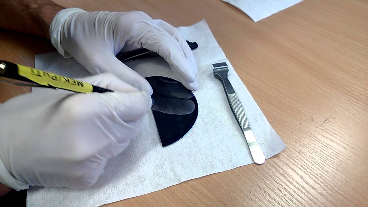
This demo shows the procedure for cleaving a silicon wafer.
si 100 wafer 주제에 대한 자세한 내용은 여기를 참조하세요.
Tấm Wafer Silicon 4Inch Loại P (100) Màng SIN 100nm <
Tấm Wafer Silicon 4Inch Loại P (100) Màng SIN 100nm <0,005Ω Chất Nền Bán Dẫn Được Đánh Bóng Đơn (1). Bấm để nhận. Giảm ₫10k.
Source: www.lazada.vn
Date Published: 3/5/2021
View: 2013
Si (510)wafer = Si (100) with 11.3 degree miscut towards <100 ...
Si (510)wafer = Si (100)) with 11.3 degree miscut towards <100><100> , 4 ” dia x 0.5 mm, 1SP, N Type (undoped, FZ R>1000 ohm-cm)
Source: www.mtixtl.com
Date Published: 6/26/2021
View: 1990
Hydrogen passivation of Si(100) wafers as templates for low …
Less is known about a similar treatment on Si(100) wafers, more commonly used in semiconductor technology. However, high temperature (T > 800°C) thermal …
Source: www.sciencedirect.com
Date Published: 12/16/2022
View: 2793
Silicon wafer single side polished, N 100, Yes phosphorus …
Silicon · wafer (single se polished), <100>, N-type, contains phosphorus as dopant, diam. × thickness 3 in. × 0.5 mm · Properties · Description · Safety …
Source: www.sigmaaldrich.com
Date Published: 10/22/2021
View: 3014
Nanopackaging of Si(100)H Wafer for Atomic-Scale … – Springer
Nanopackaging of Si(100)H Wafer for Atomic-Scale Investigations … In this way, a 200-mm wafer dicing step has been included enabling to …
Source: link.springer.com
Date Published: 4/3/2022
View: 1488
주제와 관련된 이미지 si 100 wafer
주제와 관련된 더 많은 사진을 참조하십시오 Cleaving a silicon wafer. 댓글에서 더 많은 관련 이미지를 보거나 필요한 경우 더 많은 관련 기사를 볼 수 있습니다.
주제에 대한 기사 평가 si 100 wafer
- Author: r5cpt
- Views: 조회수 25,205회
- Likes: 좋아요 95개
- Date Published: 2013. 3. 20.
- Video Url link: https://www.youtube.com/watch?v=_Rv_wTEWFdU
Si (510)wafer = Si (100) with 11.3 degree miscut towards <100>/<110> , 4 ” dia x 0.5 mm, 1SP, N Type (undoped, FZ R>1000 ohm-cm) – SiUa510ori101D05C1
Notices
2. We may add extra charges for paper order and net30 terms due to extra labor costs.
3. The prices listed are subject to change without notice.
1. Prices listed online are valid for the US market and who pay by credit card only. There will be extra charges for shipping & handling. Price various from country to country.2. We may add extra charges for paper order and net30 terms due to extra labor costs.3. The prices listed are subject to change without notice.
Silicon wafer single side polished, N 100, Yes phosphorus dopant, diam. 3in. thickness 0.5mm 7440-21-3
Our team of scientists has experience in all areas of research including Life Science, Material Science, Chemical Synthesis, Chromatography, Analytical and many others .
Contact Technical Service
Nanopackaging of Si(100)H Wafer for Atomic-Scale Investigations
Ultra-high vacuum (UHV) investigations have demonstrated a successful development of atomic nanostructures. The scanning tunneling microscope (STM) provides surface study at the atomic scale. However, the surface preparation is a crucial experimental step and requires a complex protocol conducted in situ in a UHV chamber. Surface contamination, atomic roughness, and defect density must be controlled in order to ensure the reliability of advanced UHV experiments. Consequently, a packaging for nanoscale devices has been developed in a microelectronic clean room environment enabling the particle density and contaminant concentration control. This nanopackaging solution is proposed in order to obtain a Si(001)-(2×1):H reconstructed surface. This surface is protected by a temporary silicon cap. The nanopackaging process consists in a direct bonding of two passivated silicon surfaces and is followed by a wafer dicing step into 1-cm2 dies. Samples can be stored, shipped, and in situ opened without any additional treatment. A specific procedure has been developed in order to open the nanopackaged samples in a UHV debonder, mounted in the load-lock chamber of a low-temperature STM system (LT-STM). Statistical large scan LT-UHV-SEM images and LT-UHV-STM images have been obtained enabling the surface study at the atomic resolution.
Keywords
Scanning Tunneling Microscopy
Scanning Tunneling Microscopy Image
Reduce Pressure Chemical Vapor Deposition
Scanning Tunneling Microscopy System
Scanning Tunneling Microscopy Head
These keywords were added by machine and not by the authors. This process is experimental and the keywords may be updated as the learning algorithm improves.
키워드에 대한 정보 si 100 wafer
다음은 Bing에서 si 100 wafer 주제에 대한 검색 결과입니다. 필요한 경우 더 읽을 수 있습니다.
이 기사는 인터넷의 다양한 출처에서 편집되었습니다. 이 기사가 유용했기를 바랍니다. 이 기사가 유용하다고 생각되면 공유하십시오. 매우 감사합니다!
사람들이 주제에 대해 자주 검색하는 키워드 Cleaving a silicon wafer
- silicon
- wafer
- cleaving
- microfabrication
Cleaving #a #silicon #wafer
YouTube에서 si 100 wafer 주제의 다른 동영상 보기
주제에 대한 기사를 시청해 주셔서 감사합니다 Cleaving a silicon wafer | si 100 wafer, 이 기사가 유용하다고 생각되면 공유하십시오, 매우 감사합니다.